

Revealed: The Evolution of the IC Packaging Wire Bonding Process for Future Growth
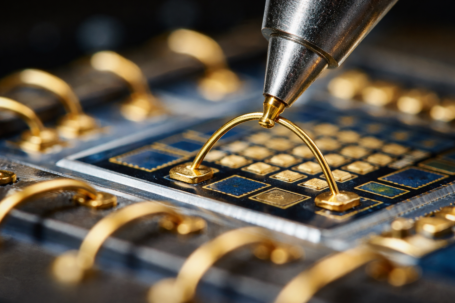
The IC packaging wire bonding process is undergoing a significant evolution, essential for the growth of various microelectronics applications. With the wire bonding market size projected to reach $8.256 billion by 2035, companies are increasingly recognizing the importance of adapting their bonding strategies to align with advancements in semiconductor wire bonding technology. The increasing demand for compact and efficient electronic devices is driving this evolution, necessitating innovative IC packaging bonding solutions to cater to a diverse range of applications.
As technology continues to advance, the need for more sophisticated microelectronics interconnect technology is becoming paramount. This shift is not only pushing the boundaries of conventional bonding methods but also reshaping the fabric of the electronics manufacturing landscape, with significant implications for future growth.
Recent developments in the IC packaging wire bonding process underscore the importance of adopting advanced packaging techniques to maintain competitive advantage. Key industry participants such as Kulicke and Soffa Industries, Inc. (US) and Microchip Technology Inc. (US) are leading innovations in the market, focusing on enhancing the reliability and efficiency of their bonding processes.
Additionally, companies like ASM International (NL) and Tokyo Seimitsu Co., Ltd. (JP) are investing in cutting-edge chip bonding equipment to ensure they meet the increasing demands of the market. The competitive landscape is further strengthened by players like Hesse Mechatronics (DE) and Shinkawa Ltd. (JP), who are introducing advanced technologies tailored for the evolving needs of semiconductor manufacturers.
Several factors drive the evolution of the IC packaging wire bonding process. The increasing demand for semiconductor wire bonding technology is at the forefront, as manufacturers seek improved performance and efficiency in their bonding operations. This demand translates into an urgent need for microelectronics bonding equipment that supports high-quality interconnects in miniaturized applications.
Yet, challenges exist within the market, particularly in adapting to rapid technological advancements. The IC packaging bonding solutions employed today must evolve to address the complexities associated with new device architectures. Furthermore, the ongoing need for precise and reliable bonding poses challenges regarding quality assurance and process optimization, which manufacturers must navigate to succeed in this competitive environment. The development of Wire Bonding Market continues to influence strategic direction within the sector.
Geographically, North America continues to dominate the wire bonding market, driven by robust investments in semiconductor manufacturing and the adoption of advanced packaging solutions. The U.S. market is particularly noteworthy, as it witnesses a surge in demand for microelectronics bonding equipment that can enhance the efficiency of the IC packaging wire bonding process.
In contrast, the Asia-Pacific region is rapidly emerging as a significant player, boasting the fastest growth rate in the wire bonding market. Countries like China and Japan are at the forefront of this surge, propelled by substantial investments in semiconductor technologies and manufacturing capabilities. This dynamic shift presents a wealth of opportunities for companies involved in semiconductor wire bonding technology and IC packaging bonding solutions.
The wire bonding market presents a plethora of opportunities, particularly in the realm of semiconductor wire bonding technology. As demand for advanced packaging techniques increases, manufacturers are encouraged to innovate and develop solutions that cater to the ever-evolving needs of the electronics industry. The IC packaging wire bonding process must adapt to accommodate new device architectures, opening doors for significant advancements in bonding methodologies.
Moreover, the increasing focus on sustainability in manufacturing practices provides additional growth avenues for companies in the microelectronics bonding equipment sector. As organizations strive to reduce their carbon footprint, the development of environmentally friendly bonding solutions presents a competitive edge in the market.
In 2022, the wire bonding market was valued at approximately $4.5 billion, reflecting a compound annual growth rate (CAGR) of around 8.5% as it moves towards the projected $8.256 billion by 2035. This robust growth can be linked to the rising integration of 5G technologies, which demand more sophisticated IC packaging solutions. For instance, companies that have adopted advanced wire bonding techniques have reported a 20% reduction in production time and a 15% increase in yield rates, showcasing the tangible benefits of innovation. The increasing complexity of devices, including wearables and IoT gadgets, necessitates greater precision and reliability in bonding solutions, driving companies to invest more aggressively in R&D.
As we move towards 2035, the IC packaging wire bonding process stands to benefit from ongoing technological advancements and market demands. The integration of AI and machine learning into bonding processes is anticipated to enhance efficiency, reliability, and cost-effectiveness. Companies that proactively embrace these advancements are expected to maintain their competitive edge and capture emerging market opportunities.
Experts project that investment in research and development will be critical to the continued evolution of the wire bonding market, allowing manufacturers to explore new applications and refine existing technologies to meet customer needs effectively.
AI Impact Analysis
Artificial intelligence is reshaping the IC packaging wire bonding process by enabling manufacturers to optimize operations through real-time data analytics. By employing AI-driven technologies, firms can enhance quality control measures, ensuring precise bonding techniques that align with the demands of modern electronic devices. Furthermore, machine learning systems can predict equipment failures, reducing unplanned downtime and increasing operational efficiency. The integration of AI within semiconductor wire bonding technology is not only streamlining processes but also paving the way for future innovations, ensuring that manufacturers remain agile in a rapidly changing market landscape.
Frequently Asked Questions
Gnss Enabled Consumer Device Market
Handheld Point Of Sale Market